Student Projects
VE/VM450
Automated Optical Inspection (AOI) in Surface Mount Processes
Sponsor: Prof. Mian Li, Foxconn Industrial Internet (Fii)
Team Members: Junyi Cheng, Haoze Hu, Fanhao Zeng, Bohao Zhang, Zehua Zhang
Instructor: Prof. Chong Han
Project Video
Team Members

Team Members:
Junyi Cheng
Haoze Hu
Fanhao Zeng
Bohao Zhang
Zehua Zhang
Instructor:
Prof. Chong Han
Project Description
Problem Statement
Foxconn Industry has many surface mount technology production lines to assemble electronic devices. Human inspection is used to ensure quality, which takes a lot of human resources. This project is to use computer vision techniques to detect components and report potential defects on PCB boards in place of human inspection.
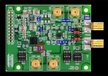
Fig. 1 Image sample of PCB board during inspection
Concept Generation
In our design, detection speed and accuracy are the two most important factors. Faster R-CNN structure is used for locating the components on PCB boards and SURF model is used to compare and match two similar images, in order to report potential defects on PCB boards.
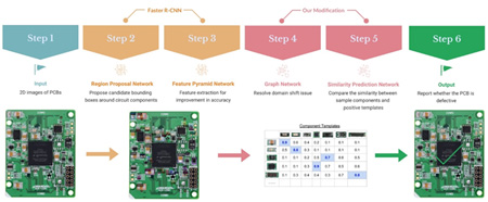
Fig. 2 Model diagram of Faster R-CNN solution
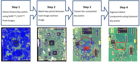
Fig. 3 Model diagram of SURF solution
Design Description
Our design compares images of PCB samples with a reference image and report potential component defects on the board and labelling their defect types. The entire problem is decomposed into two sub-functions: defect localization and defect classification. By utilizing both SURF model and Faster R-CNN structure, two subsystems are built to handle each sub-function individually and the outputs of the two subsystems are combined in the last stage to provide the results.
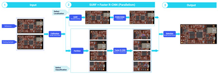
Fig. 4 Concept Diagram of the AOI system
Implementation Details
A Python program implementing the above algorithms is built to detect the defects on PCB boards. It firstly read in an image and try to locate the defects.
Then it will use structural similarity index (SSIM) and the peak signal-to-noise ratio (PSNR) to get rid of the false positives.
With the information of the locations of the defects and the deep-learning model we have trained, we then can determine the defect types we have on the input PCB image.
Finally, we will summary the results of the detection and output some texts in the terminal.
The whole program will run in approximately 10 seconds.
Validation
Validation Process:
We have prepared a test dataset with functioning and defective PCB images arranged randomly in order to validate that our design can satisfy the engineering specifications.
All the defective samples are generated and labelled manually by us using Photoshop and Labelme.
We have controlled the distribution of defect types in our test dataset to resemble the distribution provided by Fii to mimic the real-world situation at Fii’s assembly line.
Validation Results:
√ Average precision > 80%
√ Detection speed > 30 cm2/s
√ Missing components (missing rate < 5%)
√ Wrong components (missing rate < 5%) √ Precision of defects for each circuit component category > 80%
• Universal solution
√ means having been verified and · means to be determined.
Conclusion
Computer vision techniques can be used to detect defects on PCB boards. The key to achieve this goal is to develop accurate, robust and efficient algorithms. Also, the interpretability and universality of the algorithm is also important. In this project, we have proposed a well-formed algorithm and an elegant implementation.
Acknowledgement
Sponsor: Dr. Baoyang Jiang and Chao Sun from Foxconn Industrial Internet
Prof. Chong Han and Prof. Mian Li from UM-SJTU Joint Institute
Reference
[1] Ren, Shaoqing, et al. “Faster R CNN: Towards Real Time Object Detection with Region Proposal Networks.” IEEE Transactions on Pattern Analysis and Machine Intelligence, vol. 39, no. 6, pp. 1137-1149, 1 June 2017.