The classical photoconductor gain theory may be revolutionalized, thanks to research finding of Professor Yaping Dan’s team at the University of Michigan-Shanghai Jiao Tong University Joint Institute (UM-SJTU JI). The research finding was published recently in an article entitled “Explicit Gain Equations for Single Crystalline Photoconductors” in ACS Nano.
The research article reveals the high gain of photoconductors originates from the conducting channel width modulation by light illumination. Based on this mechanism, the team further derived explicit gain equations which can fit well with the experimental data. Professor Yaping Dan is the corresponding author. Ph.D student Jiajing He and Ph.D graduate Dr. Kaixiang Chen are the co-first authors, Ph.D student Xiaoming Wang from the joint institute, Professor Yongning He and Master student Chulin Huang from Xi’an Jiao Tong University also participated this research work.
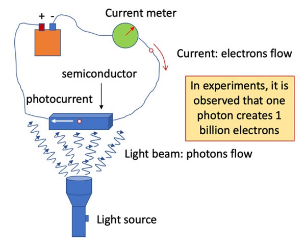
Photoconductors is one of the simplest devices consisting of a resistor in contact with two metal electrodes at the terminals. It was observed in experiments that photoconductors often have extraordinarily high photo gains. The gain sometimes is as high as 1 billion, which means 1 billion electrons can be generated for every photon that the semiconductor absorbs.
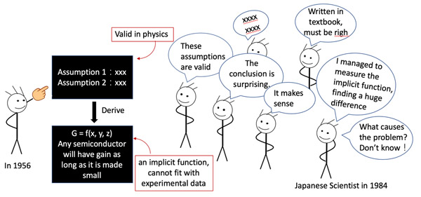
In 1956, R. L. Petritz derived a gain theory for the gain mechanism (written in the classical textbooks on semiconductor physics and devices), stating that a photoconductor will intrinsically have an extraordinarily high gain as long as the minority carrier lifetime is long and the carrier transit time is short enough by making the device short. However, the minority carrier lifetime is difficult to calibrate, in particular for low dimensional semiconductors. Therefore, the classical gain theory is inexplicit since it cannot fit with experimental data in which the photo gain is often plotted as a function of light intensity and device physical parameters. In 1980s, Japanese scientist Nozomu Matsuo and coworkers managed to calibrate the minority carrier lifetime in GaAs thin films, finding that the gain predicted by the classical theory was smaller than the values measured in experiments by 3-4 orders of magnitude. In the following decades, other scientists also found that the classical theory was problematic. But no one ever pointed out what was wrong with the classical theory and what would be the correct theory.
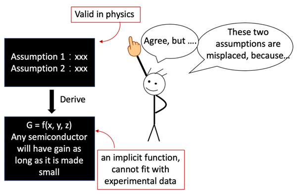
In 2018, Professor Dan and his team published two research articles in ACS Photonics and ACS Nano, pointing out that the classical gain theory was derived on two displaced assumptions. The first assumption is uniform distribution of excess electrons and holes in photoconductors which is invalid due to the confinement of metal-semiconductor boundary. The second assumption is that the number of photogenerated electrons and holes contributing photoconductivity are equal, which is only true in “ideal” semiconductors. In real semiconductors, there are always defects and potential wells that will localize excess minority carriers, resulting in the inequality of excess electrons and holes in the conduction channel.
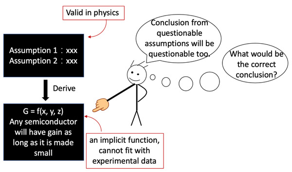
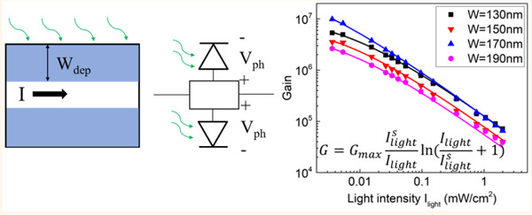
In this publication, Professor Dan and his team found that photogain of the photoconductors originates from the widening of the conducting channel thanks to the accumulation of photogenerated majority carriers in the conduction channel. A high-gain photoconductor can be modeled as a resistor modulated by floating Schottky junctions. Base on this, the team further derived the explicit gain equations which can fit well with the experimental results. These gain equations can predict the performance and guide the design of high-performance photoconductors. These gain equations can also be employed as material characterization methods allowing for the extraction of parameters such as minority carrier lifetime, surface recombination velocity that are normally difficult to calibrate.
Links to the research article
Explicit Gain Equations for Single Crystalline Photoconductors
Jiajing He, Kaixiang Chen, Chulin Huang, Xiaoming Wang, Yongning He, Yaping Dan*
ACS Nano 18 (2020) accepted.
https://pubs.acs.org/doi/pdf/10.1021/acsnano.9b09406
Background Information
 Yaping Dan is currently a tenure-track associate professor at the UM-SJTU Joint Institute. He received his Bachelor’s degree from Xi’an Jiao Tong University in 1999, Master’s degree from Tsinghua University in 2002, and Ph.D. degree from the University of Pennsylvania in 2008. He conducted his postdoctoral research at Harvard University from 2008 to 2012 before joining the joint institute in 2012. His research interests focus on fully integrated all-silicon photonics and single atom electronics, aiming to provide key technological solutions to advanced integrated circuits and quantum computing.


